¿qué estás buscando??
Búsquedas populares
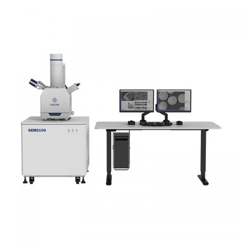
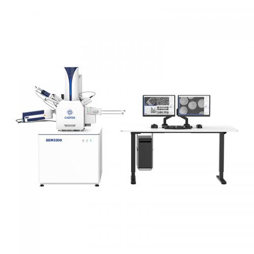
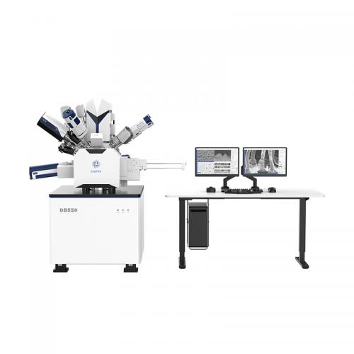
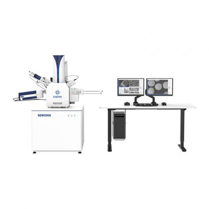
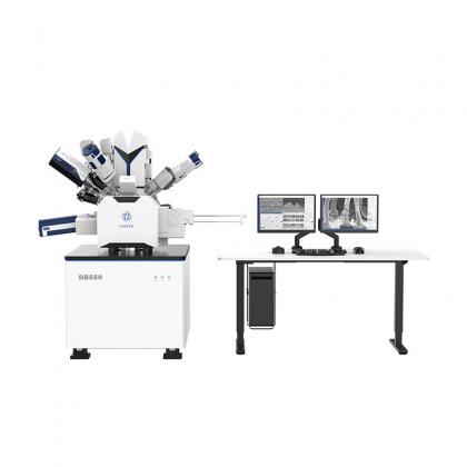
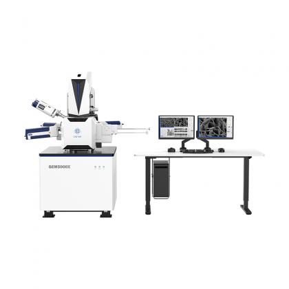
- Proveedor global del fabricante del microscopio electrónico de barrido de emisión de campo
- Detectores SEM EDX, EDS, EBSD, BSE, CL, STEM
- Aplicaciones QDAFM del microscopio de fuerza atómica del diamante cuántico del magnetómetro NV de escaneo
- Fabricante de microscopio central NV de escaneo ciqtek
- Proveedor global de magnetometría NV de escaneo
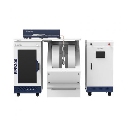
- Proveedor global de espectroscopia de resonancia paramagnética electrónica de pulso de banda X
- Espectroscopia de resonancia paramagnética electrónica al mejor precio
- Espectroscopía EPR de banda X con criostato
- Espectroscopia de resonancia paramagnética electrónica de banda W al mejor precio
- Espectroscopia de resonancia de espín electrónico de banda W al mejor precio